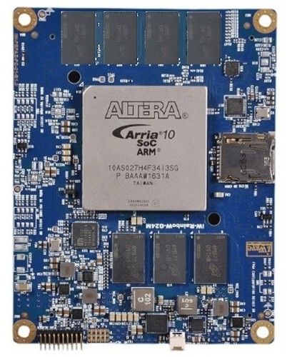
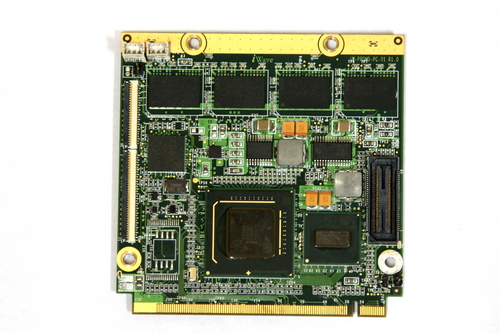
Brass Arria 10 Soc System On Module
Get Latest Price
In Stock
Product Specifications
| Connectors | Dual 240-pin |
| Dimensions | 95mm x 75mm |
| FPGA IOs | Upto 76 LVDS |
| Features | High speed, Dual core, DDR4 support, Versatile IOs, Industrial grade, Compact form, Scalable design |
| Memory | 1GB DDR4 |
| Power | 5V |
| SoC/FPGA | Arria 10 SoC/FPGA |
| Transceivers | 24 @ 17.4Gbps |
Product Overview
Key Features
Highlights:
Arria10 SoC & FPGA device compatibility
SX270, SX320, SX480, SX570, Sx660
Gx270, GX320, GX480, GX570, Gx660, GX900, GX1150
24 high speed transceivers @ 17.4Gbps
Up to 76LVDS/152SE FPGA IOs
8LVDS/8SE General purpose clock outputs
7LVDS/7SE General purpose clock inputs
64 - Bit DDR4 support for FPGA
Dual 240 Pin Board to Board Connector
Variable IO voltage support
Industrial Grade operation
Specification:
SoC/FPGA:
Intel Arria10 SoC/FPGA
Compatible Arria10 SoC Family - SX270, SX320, SX480, SX570, SX660
With upto 660K Logic Elements, 24 High Speed Transceivers and integrated Dual Core ARM Cortex A9 @ upto 1.5 GHz/Core Hard Processor System (HPS).
Compatible Arria10 FPGA Family - GX270, GX320, GX480, GX570, GX660, GX900, GX1150
With upto 660K Logic Elements and 24 High Speed transceivers
Memory:
1GB DDR4 SDRAM (32bit) with ECC for HPS/FPGA (Expandable) A , A
MicroSD Connector for HPS booting A , A
NAND Flash for HPS booting (Optional) A , A
Configuration Flash for FPGA (Optional)
DDR4 RAM (64bit) from FPGA (Optional)4
Other On-SOM Features:
JTAG Header
FAN Header
FPGA AS Header (Optional)
FPGA Configuration Selection Switch (Optional)
Board to Board 1 Interfaces:
FPGA High Speed Transceivers (upto 17.4Gbps) x 18
FPGA IOs & General Purpose Clocks - Bank2A
Upto 46 Single Ended IOs
One General Purpose Clock Input LVDS Pair/Single Ended
Two General Purpose Clock Output LVDS Pairs/Single Ended
FPGA IOs & General Purpose Clocks a Bank3A
Upto 47 Single Ended IOs
Two General Purpose Clock Input LVDS Pairs/Single Ended
Two General Purpose Clock Output LVDS Pairs/Single Ended
Board to Board 2 Interfaces:
From HPS Block: 1, 5
Gigabit Ethernet x 1 Port (through On-SOM Gigabit Ethernet PHY)
USB OTG x 1 Port (through On-SOM USB ULPI PHY)
Debug UART (UART0) x 1 Port
Data UART (UART1) x 1 Port (With CTS & RTS)
SPI x 1 Port
I2C x 1 Port
HPS GPIOs
HPS Warm Reset
From FPGA Block:
FPGA High Speed Transceivers (upto 17.4Gbps) x 6
FPGA IOs & General Purpose Clocks a Bank3B
Upto 24 LVDS IOs
Two General Purpose Clock Input LVDS Pairs/Single Ended
Two General Purpose Clock Output LVDS Pairs/Single Ended
FPGA IOs & General Purpose Clocks a Bank3C
Upto 24 LVDS IOs
Two General Purpose Clock Input LVDS Pairs/Single Ended
Two General Purpose Clock Output LVDS Pairs/Single Ended
JTAG Interface
Power Supply: 5V
Form Factor: 95mm x 75mm
REACH & RoHS Compliant
A In Arria10 SoC/FPGA SOM, these interfaces can be supported only if Arria10 SoC family devices which supports Hard Processor System (HPS) are used.
A In Arria10 SoC/FPGA SOM, if Arrai10 SoC family device is not used and FPGA family device is used, then also 32bit DDR4 can be supported from FPGA fabric.
A In Arria10 SoC/FPGA SOM, these interfaces can be supported only if Arria10 SoC family devices are used because these interfaces are supported through Dedicated I/O pins of Hard Processor System (HPS).
4 Supported on SX480/GX480 or higher family devices only.
5 In Arria10 SoC/FPGA SOM, if Arrai10 SoC family device is not used and FPGA family device is used, then these Shared I/O interfaces cannot be used. But the same pins can be used as FPGA Bank2L from FPGA fabric.
Company Details
Business Type
Service Provider
Employee Count
120
Establishment
2001
Working Days
To
Related Products
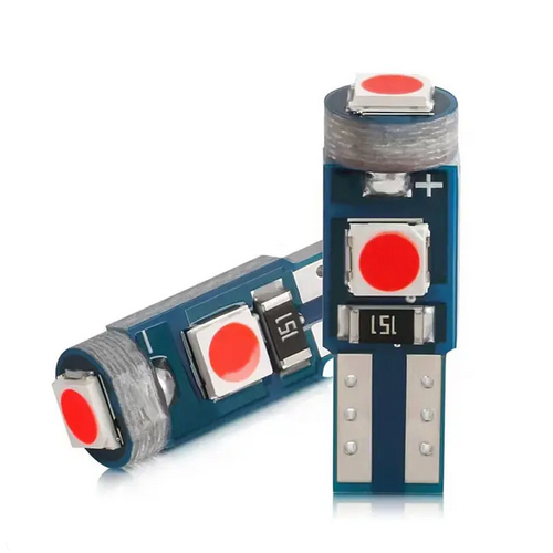
T5 Wedge Led Bulb 3030 3Smd For Car Auto Dashboard Life Span: 12 Months
MOQ - 10 Piece/Pieces
Guangzhou Liwin Co., Ltd
Guangzhou, Guangdong


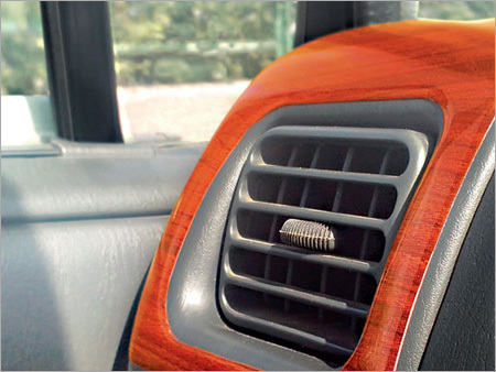
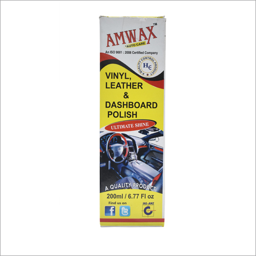
Auto Dashboard Cleaner Wax Spray Cockpit Detailer 500ml - Spray, 3 Years Expiration | Cleans & Protects ABS, Plastic, Vinyl, Rubber Interiors
Price: 0.93-0.99 USD ($)
MOQ - 7500 Piece/Pieces
Shenzhen I-like Fine Chemical Co., Ltd
Shenzhen, Guangdong

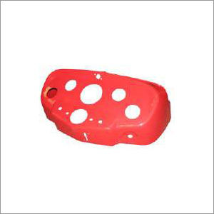
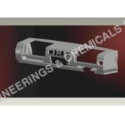
Auto Dashboard - Mild Steel, Polished Finish, 200 MPA Tensile Strength | Hot Rolled for Four Wheelers
Price: 1000 INR
MOQ - 500 Unit/Units
Rydot Infotech
Sanand, Gujarat


Explore Related Categories


More Products From This Seller


Seller Details
Bengaluru, Karnataka
Name
Fathima
Address
7/B, 29th Main, BTM Layout 2nd Stage, Bengaluru, Karnataka, 560076, India
auto dashboard in Bengaluru
Report incorrect details