

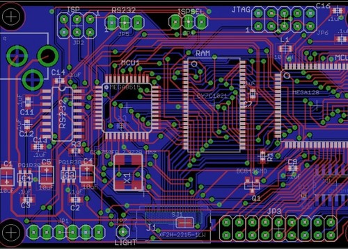
Pcb Designing Course
Price:
Get Latest Price
Brand Name :
Nano Scientific Research Centre
In Stock
Product Specifications
| Certification | Yes/No |
| Course Duration | Variable |
| Delivery Method | Online |
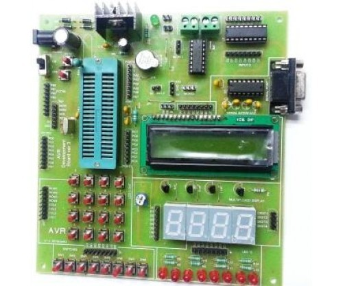
| Features | PCB Design, Schematic Capture, Component Placement, Routing Techniques, Manufacturing Process, PCB Etching, Symbol Recognition, Footprint Identification |
| Learning Outcome | PCB design proficiency |
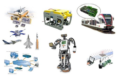
| PCB Technologies Covered | Analog, Digital, RF |
| Software Used | Range |
| Usage | Learn PCB design, schematic capture, component placement, routing techniques, and manufacturing processes. |
| Payment Terms | Others, Cheque |
| Main Domestic Market | Telangana |
Company Details
Established in 2008, Nano Scientific Research Center Pvt. Ltd. has made a name for itself in the list of top service providers of Coaching Institutes in India. Nano Scientific Research Center Pvt. Ltd. is listed in Trade India's list of verified companies offering a wide array of 8051 Microcontroller Course, ARM 7 Course, Advance Diploma Course In Asic Design & Verification, etc. Contact here for Coaching Institutes in Hyderabad, Telangana.
Business Type
Service Provider
Employee Count
28
Establishment
2008
Working Days
To
More Products From This Seller


Seller Details
Hyderabad, Telangana
Director
Mr. Aravind Reddy
Address
4 & 6th Floor, Siri Estates, Opposite To Karur Vysya Bank, Opposite Lane To R.S. Brothers, Ameerpet Hyderabad, Telangana, 500073, India
pcb design services in Hyderabad
Report incorrect details


