

Pcb Design Services In Hyderabad
(109 products)

PCB Design Services - Ultra-High Density Up to 30 Layers | High-Speed Digital Analog Mixed-Signal Designs Fast Turnaround Standards Compliant
SoftwareMentor Cadence Altium
LayersUp to 30
Speed2.5 Gbps+
DensityUltra-high
StandardsIPC UL MIL
UsagePCB design for diverse electronics
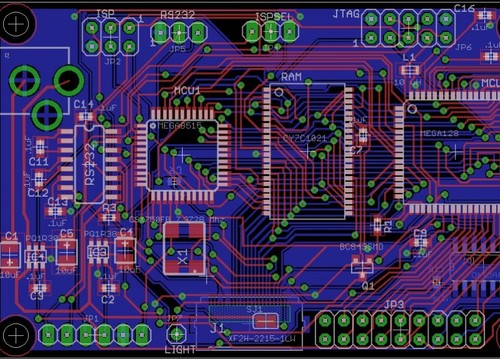
PCB Designing Course
Course DurationVariable
Delivery MethodOnline
Software UsedRange
PCB Technologies CoveredAnalog Digital RF
Learning OutcomePCB design proficiency
CertificationYes/No

PCB Design Services - High Current Power Supply High-Speed BGA Routing & Fine Pitch Designs | Comprehensive Documentation & Industry-Leading Tools
SoftwareCadence Allegro Mentor Graphics Cadence Star
Design TypesHigh-speed High-voltage Power Supply
Component SupportBGAs Fine pitch
DeliverablesComplete documentation Gerber files
Revision ControlVersion control systems
AnalysisSignal Integrity EMI/EMC

Pcb Designing Services Efficacy: Promote Growth
Design SoftwareAltium
File FormatsMultiple
Revision ControlGit
ManufacturingSupport
TestingIncluded
UsageIndustrial PCB design prototyping and manufacturing support.
Hidden View Solutions Pvt Ltd
Madhapur, Hyderabad

Power Supply PCB Design Service - FR4 Material 2-4 Layers Custom Designs PCB Expertise Power Solutions Reliable and Efficient Designs
Design TypeCustom
TechnologyCAD/CAM
PCB MaterialFR4
Layers2-4
ComplianceIEC
UsagePower supply design for AC-DCDC-DC converters and battery chargers

PCB Design Services - Up to 20 Layer FPGA Based Digital and Analog Memory Design | Expert Level Quality Market Leading Price
Layers1-20
Design TypesAnalog Digital
SoftwareAltium Eagle
ComplianceIPC-2221
Turnaround Time1-4 weeks
UsagePCB design for various electronic applications including FPGA-based systems and complex multi-layer boards.

PCB Design Development Services - FR4 Green CAD/CAM | Custom Design Project-Based 2-3 Days Completion
Design SoftwareCAD/CAM
Service ContractProject-based
Turnaround Time2-3 days
PCB MaterialFR4
ColorGreen
UsageAudio amplifier circuit design

Full Custom PCB Design Services
Design TypeFull Custom
MaterialFR4
Layers2-10
Surface FinishHASL
Minimum Track Width5 mil
UsagePrototyping and low-volume production

PCB Design Services - High-Quality Components | Customized Solutions by Experienced Professionals
Design SoftwareAltium
PCB MaterialFR4
Layer Count4-12
Minimum Trace Width0.1mm
ComplianceIPC-A-600
UsageElectronic product design and manufacturing prototyping and testing.
Continent Trading & Consulting
Ahilyanagar
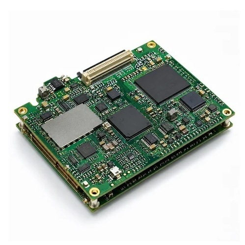
Pcb Design Service
Price: 2000 INR/Piece
MOQ1 Piece/Pieces Piece/Pieces Piece/Pieces Piece/Pieces Piece/Pieces Piece/Pieces
Payment TermsCash in Advance (CID) Cheque Others Telegraphic Transfer (T/T)
Supply Ability25 Per Day
Delivery Time4 Days

PCB Design (Schematic Capture and Layout Design) - FR4 Rogers 2-12+ Layers IPC-2221A | High-Speed Routing DFM Prototyping Manufacturing Support
Design SoftwareAltium Eagle
Layers2-12+
Trace Width5-50 mil
Board MaterialFR4 Rogers
ComplianceIPC-2221A
UsageElectronics prototyping embedded system development product manufacturing
Radifonics Solutions Private Limited
Binnamangala, Bengaluru

PCB Design Services - High Complexity IPC-A-600 Compliant | Efficient Custom Designs Advanced Testing Single/Double-Sided Boards
Design SoftwareAltium Eagle
LayersSingle/Double sided
Manufacturing ProcessSMT THM
Turnaround Time1-4 weeks
Compliance StandardsIPC-A-600
UsagePCB design for Bengaluru & Karnataka
FAQs Related to Pcb Design Services In Hyderabad
How many pcb design services products are available in Hyderabad?
Where can I find pcb design services nearby Hyderabad?
What are some related categories to pcb design services in Hyderabad?
Can I trust the Hyderabad Based Pcb Design Services suppliers listed on Tradeindia?
How many Hyderabad based Pcb Design Services manufacturers are there?
What is the price range of pcb design services in Hyderabad?
| Company Name | Currency | Product Name | Price |
|---|---|---|---|
| - | - | PCB Designing Course | nan INR (Approx.) |
| - | - | PCB Designing Services | 10 INR (Approx.) |
| - | - | Full Custom PCB Design Services | 250 INR (Approx.) |
| - | - | Pcb Design Service | 2000 INR (Approx.) |
What is the delivery time for pcb design services in Hyderabad?
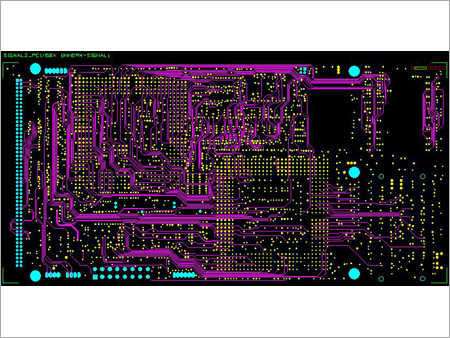
PCB Design Inner layer
MaterialFR4
LayersMulti-layer
Thickness1-10mm
DimensionsCustomizable
Trace Width5-50mil
UsagePCB inner layer for complex electronic circuits. Used in high-reliability applications.

PCB Cad Design Services - FR4 Material Custom Size Multiple Layers Utilizing Altium Software | Accurate Designs Expert Engineers Fast Turnaround
SoftwareAltium
LayersMultiple
MaterialFR4
SizeCustomizable
ThicknessVariable
Trace widthVariable
S. B. Technologies
Kanakapura Main Road, Bengaluru

PCB Design Services - 2-16 Layer Custom Printed Circuit Board Design | IPC-2221A Compliance Fast Turnaround Reliable Service Expert Design Using Altium & Eagle
Design SoftwareAltium Eagle
Layer Count2-16 layers
Manufacturing MethodSMT THM
File FormatsGerber ODB++
Revision ControlGit
UsageElectronic device creation prototyping and production

Attractive PCB Design Services - FR4 & Rogers
Design SoftwareAltium
Layers4-12
MaterialsFR4 Rogers
Size Range1-100cm²
ManufacturingIPC-A-600
UsagePrototyping and production of PCBs for various electronics applications.
Rms Technologies Pvt. Ltd.
Jayanagar, Bengaluru

PCB Design Service - FR4 Material 1.6mm Thickness Custom Size | Advanced Tools Expert Engineers Fast Turnaround Reliable Designs
MaterialFR4
LayersMultiple
Trace widthVarious
Surface finishHASL
Thickness1.6mm
SizeCustomizable

PCB Design Services - Expertly Crafted For Reliable Electronic Component Support | Low Maintenance Cost-Effective Solutions
Design SoftwareAltium Eagle
Layers2-20+
Board Size10mm-500mm
TechnologySMT THM
ComplianceIPC-2221
MaterialsFR4Rogers
Microwave Tech Products
Magadi Road, Bengaluru

Hardware And Board Design Service
Design SoftwareAltium Eagle
Board MaterialFR4 Rogers
Layer Count2-16 layers
Manufacturing ProcessSMT THM
ComplianceRoHS CE
Turnaround Time1-4 weeks

Pcb Design Service - IPC-2221A Compliance 2-32 Layers Altium & Eagle Support | Fast Turnaround Expert Design Customer Collaboration
SoftwareAltium Eagle
Design TypesAnalog Digital
Layers2-32
RevisionsUnlimited
Turnaround Time1-4 Weeks
UsageElectronic prototype design PCB layout schematic creation and manufacturing file generation for various electronic devices.
Jupiter Design Technologies Pvt. Ltd.
Lavakusha Nagar, Bengaluru

Complex PCB Design Services - FR4 Copper Multilayer Custom Thickness HASL ENIG Finish | Precise Operation Organized Design Error-Free Client-Centric Easy Upgrade
MaterialsFR4 Copper
LayersMultilayer
DimensionsVariable
ThicknessCustomizable
Surface finishHASL ENIG
Impedance controlAvailable

PCB Design Service - Tailored Solutions for High-Quality Circuit Boards Experienced Experts Timely Delivery
Design SoftwareAltium Eagle
Layers2-32 layers
File FormatsGerber ODB++
Compliance StandardsIPC-2221
Revision ControlVersion control
Turnaround Time1-4 weeks
Tessolve Semiconductors
Doddathoguru, Bengaluru

PCB CAD Design Services
SoftwareAltium Eagle
Design ComplexityHigh/Medium
Layers2-16
RevisionsUnlimited
Turnaround Time2-4 weeks
UsagePCB design schematic capture PCB layout and board procurement in Bengaluru Karnataka India
Kaynes Technology India Pvt. Ltd.
Peenya, Bengaluru

Pcb Designs Service
Design SoftwareAltium
PCB MaterialFR4
Layers2-8
Minimum Trace Width0.1mm
Surface FinishHASL
UsageIndustrial solutions academic projects training

PCB Design and Layout Services
SoftwareProtel OrCAD AutoCAD
LayersMulti-layer
Design Rule CheckYes
Output FormatsGerber PDF
Revision ControlYes
UsagePCB design & layout for various electronic products.

PCB Design services
LayersMultilayer
Design TypesAnalog Digital
SoftwareAltium Eagle
Turnaround1-4 weeks
UsageElectronic device prototyping industrial applications consumer electronics medical devices automotive applications.
ComplianceIPC

PCB Design Software Service
SoftwareDipTrace
Design TypeMulti-layer
SchematicHierarchical
RoutingAutorouter
VerificationReal-time DRC
Export FormatsMultiple
Popular Categories in Hyderabad



© 1999-2026 Infocom Network Private Limited. All rights reserved.