
Hdi Green Solder Mask Osp Printed Circuit Board
Price: 1 USD
Get Latest Price
Minimum Order Quantity :
1
In Stock
Product Specifications
| Thickness | 0.1mm-5mm |
| Linewidth | 0.075mm/3mil |
| Gap | 0.065/2.8mil |
| Aperture | 0.15mm/0.45mm |
| BGA | 0.2mm |
| Layers | 4 layers |
| Screen | 36t |
| Features | High Density, Green Solder Mask, OSP Finish, Fine Lines, Reliable BGA, Precise Circuits, Durable, Cost-effective |
| FOB Port | Customer settings |
| Payment Terms | Letter of Credit at Sight (Sight L/C), Telegraphic Transfer (T/T), Paypal |
| Supply Ability | 80000 Per Week |
| Delivery Time | 30 Days |
| Packaging Details | Customer settings |
| Main Export Market(s) | Asia, Australia, Central America, North America, South America, Eastern Europe, Western Europe, Middle East |
Product Overview
Key Features
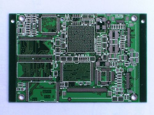
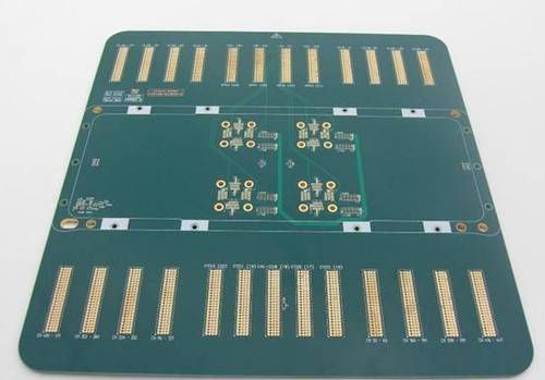
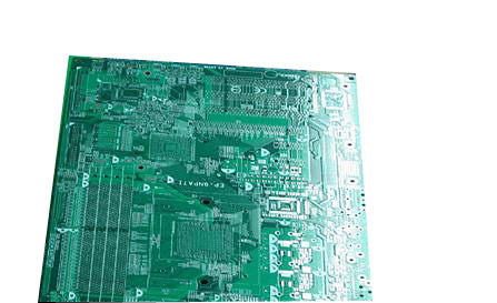
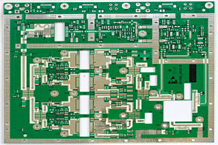
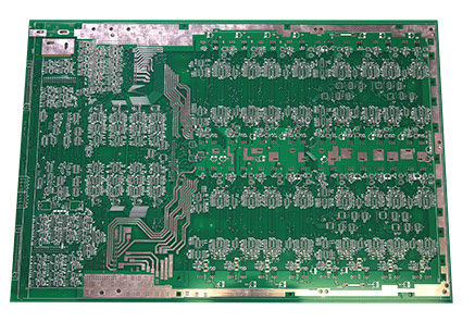
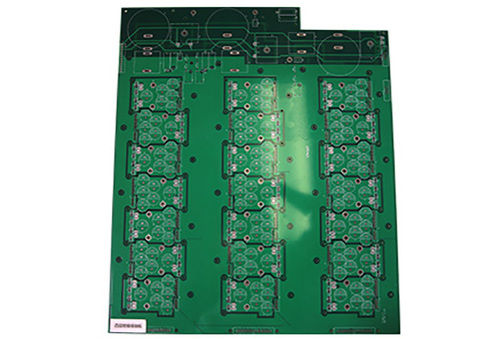
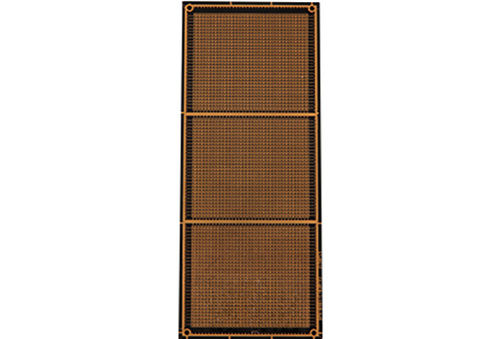
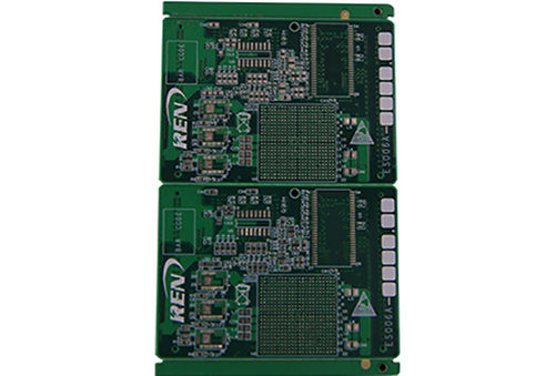
Our provided product is HDI Green Solder Mask OSP Printed Circuit Board.
HDI green solder mask OSP printed circuit board
Green solder mask PCB, OSP printed circuit board
1)A Thickness : 0.1mm-5mm
2)A Minimum linewidthi 0.075mm/3mil
3)A Minimum gap i 0.065/2.8mil
4)A Minimum apertureA inradium i 0.15mm
5)A Minimum aperture external diameter i 0.45mm
6)A Minimum BGA : 0.2mm
7)A Layer i 4 layers through hole non-impedanceA
All multilayer boards are printed with 36t screen, the resistance welding oil is 50 tons thicker than the traditional 43t, which provides reliability guarantee for the bga and more precise fine lines.
Company Details
HK CT TECH CO.,LIMITED(Shenzhen Shengxu Electronics Technology Co.,Ltd.) is a manufacturer who provides pcb proofing and production, pcba manufacturing and materials purchasing, finished products assembly and production of one-stop service for global customers. CTT committed to provide first-class services for global enterprises, to create business value for our customers. Our company is located in Shenzhen Shiyan Tangtou Hongfa Technology Park, pcba processing plant area 2500 m2A A A A A A employees more than 150 people. Owns the smt machine room, the automatic flowing plug-in lines, the wave- soldering, the automatic constant temperature tin holding tools, average daily capacity of 400000 units dip plug-in ability; Total 4 assembly line, more than 3 million points per working day processing capacity which can adapt to large, medium and small equipment products assembly; With bga mounting technology and repair technology, with 100 square meters of high temperature aging room, ultrasonic cleaning room, complete anti-static production measures, dust-free production workshop. The PCB production plant area is 5000 m2A A A A A A which can produce 20 layers multilayer PCB.The minimum aperture could be 0.15mm, minimum linewidth / gap 2.8mil. The average monthly output is 8000 square meters and the average monthly sample is 1500 models. Our main business is pcb proofing and production, smt processing, patch processing, plug-in processing, post welding processing, template welding, bga mounting, bga rework, bga bead planting, testing, finished product assembly, finished product aging, finished product packaging.
Business Type
Exporter, Manufacturer
Employee Count
200
Establishment
2008
Working Days
Monday To Sunday
Related Products

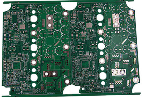
Multilayer PCB - High Grade Material, Custom Specifications for Versatile Applications
Andwin Circuits Co.,ltd
Shenzhen, Guangdong

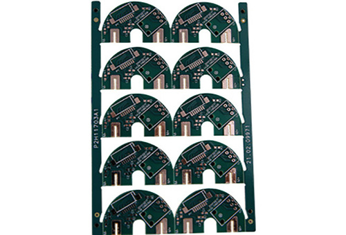
Professional Multi Layer Oem Fr4 Pcb Circuit Board
Airuida Technology Co., Limited
Shenzhen, Guangdong

Explore Related Categories


More Product From This seller
Seller Details
Shenzhen, Guangdong
Mr Edward
Address
5th Floor, Building F, Hongfa Technology Industrial Park, Tangtou Community, Shiyan Street, Baoan District, Shenzhen, Guangdong, 518000, China
multilayer pcb in Shenzhen
Report incorrect details