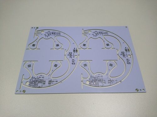
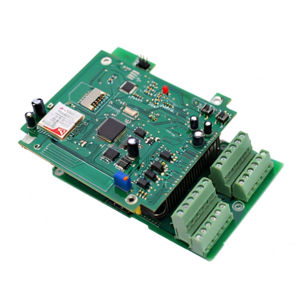
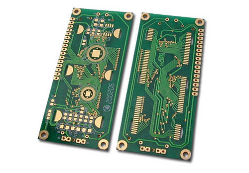
Electronic Pcba Prototyping - Advanced Material Options, Max Size 1200x2000mm, Precision Tolerance ±0.05mm | Smd & Tht Assembly, Buried & Blind Vias, Controlled Impedance
Price:
Get Latest Price
In Stock
Product Specifications
| Copper Thickness | 0.5oz-5oz |
| Dimensions | Variable |
| Features | Rapid Prototyping, High Reliability, Customizable Designs, SMD & THT, Cost-effective, Quick Turnaround, Versatile Materials |
| Hole Size | 0.075mm |
| Materials | FR4, Aluminum |
| Max Size | 1200x2000mm |
| Thickness | 0.25-6.00mm |
| Trace Space | 0.075mm |
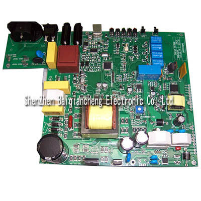
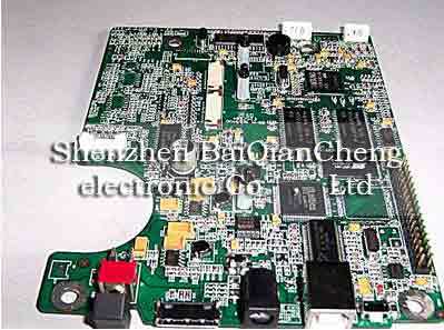
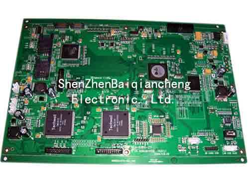
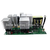
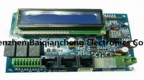
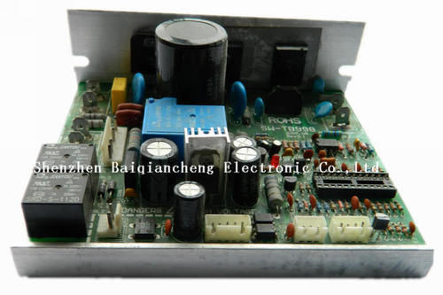
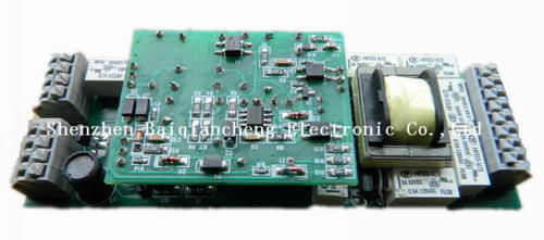
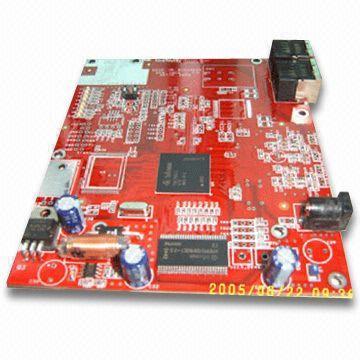
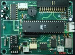
Product Overview
Key Features
1. Surface Mounted Technology Assembly (SMD)
2. Through Hole Technology Assembly (THT)
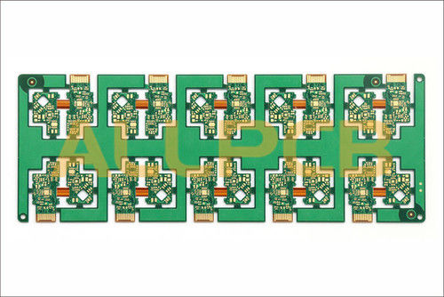
3. Profiling: Punching, Routing, V-cut, Beveling
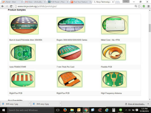
4. Material based: CME1, CME3, FR4, High TG FR4, Halogen-free FR4, Aluminum, Ceramic, PTFE(F4B, F4BK), Rogers(4003, 4350, 5880), Taconic, Arlon(35N, 85N), etc.
5. Max. size: 1200mm*2000mm
6. Board Thickness: 0.25-6.00mm
7. Min. Trace Space: 0.075mml
8. Min. Laser Hole Size: 0.075mm
9. Copper Thickness: 0.5oz-5oz
10. Min.hole ring: 0.075mm
11. Hole position/Tolerance: A 0.05mm / A 0.075mm
12. Special requirements: Buried & Blind vias + Controlled impedance + BGA
Company Details
Business Type
Exporter, Manufacturer, Service Provider, Supplier
Establishment
2000
Related Products

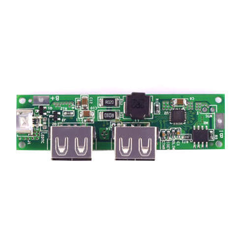
4x6cm Double Side Prototype PCB Universal Printed Circuit Board S7NF
Shenzhen Telionpcb Electronic Co., Ltd.
Shenzhen, Guangdong

Energy Storage Systems Ess Prototype Pcb Assembly Base Material: Fr4
Price: 10 USD ($)
MOQ - 2 Square Meter/Square Meters
Shenzhen Grande Electonics Co. Ltd.
Shenzhen, Guangdong
China PCBA one stop Manufacture PCB Assembly Fast PCBA Service Prototype PCB Assembly supplier
MOQ - 1 Piece/Pieces
Nova Technology Vietnamese Company Limited
Ho Chi Minh City, Thanh Pho Ho Chi Minh
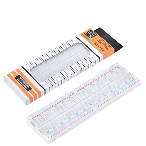
MB102 - ABS Material Prototype Breadboard , 830 Points High Quality , White Color , 1 Year Warranty
Price: 47 INR
MOQ - 1 Piece/Pieces
Robotics Embedded Education Services Private Limited
New Delhi, Delhi
Multilayer Prototype PCB - FR4 Material, Custom Dimensions, Multiple Layers | Fast Prototyping, HASL Finish, On-Time Shipping
Prism Circuitronics Private Limited
Mumbai, Maharashtra
Prototype Printed Circuit Board - FR-4, 1.6mm Thickness, 10mil Spacing | Compact Size, Easy Maintenance, Quick Turnaround, High Durability, Versatile Design
Sunanda Enterprises
Navi Mumbai, Maharashtra
2 Layer Prototype PCB Board - FR4 Material, 25x80mm Size, Green Color, 1oz Copper Thickness, 0.3mm Hole Size, 50V Impedance | ENIG Surface Finish, Lead-Free, White Silkscreen, E-Test Warranty 2 Years
Price: 5 USD ($)
MOQ - 5 Piece/Pieces
All Pcb
Hangzhou, Zhejiang
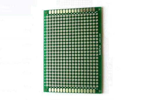
5x7cm Size 1.6mm Thickness Double Side Prototype PCB Universal Board - FR4 Epoxy Glass, Green Color, 5 Layers, Lead-Free Surface Finish, Reusable
Price: 35 INR
MOQ - 500 Piece/Pieces
Suman Electronics
Patna, Bihar
Explore Related Categories


More Products From This Seller
Seller Details
Shenzhen, Guangdong
Name
Ms. Lala Zhang
Address
null Shenzhen, Guangdong, 518128, China
prototype pcb in Shenzhen
Report incorrect details