

Electronics Design Process In Mysuru
(169 products)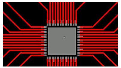
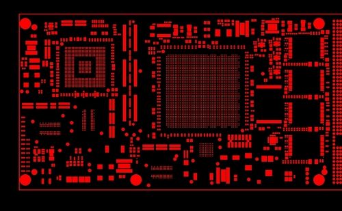
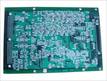
PCB Layout Design Service - High Density Up to 32 Layers | Analog Digital Mixed Designs DFM & DFT Focus
ComplianceIPC-2221
Design TypesAnalogDigitalMixed
FeaturesHigh Quality Fast Turnaround Reliable Service Expert Design DFM Focused Cost Effective
Layer CountUp to 32
Package TypesBGAQFNSOIC
SoftwareAltium Eagle
Electronics Designing Services - Reliable and Cost-Effective Solutions | Best in Class Quality International Expertise Customized Manufacturing
ComplianceIEC
Design TypeCustom
FeaturesCost-effective Reliable solutions High quality Top performance
RevisionsUnlimited
SupportFull cycle
TechnologyDigital

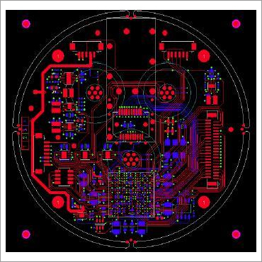
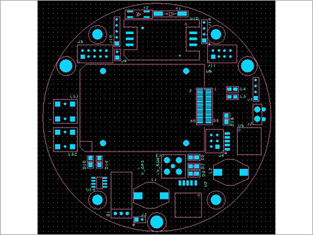
PCB Layout Design - High-Speed Multi-Layer 30 Layer IPC Compliant | Advanced Signal Integrity Analysis Impedance Control Ultra High Density
AnalysisSignal Power Thermal
BGA0.5mm pitch
FeaturesHigh-speed design Multi-layer PCB Fast turnaround High quality Cost effective
LayersUp to 30
SoftwareMentor Cadence
Speed2.5Gbps
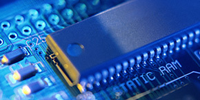
Pcb Design
Board SizeVariable
ComplianceIPC-2221A
Design SoftwareCadence Allegro Mentor Graphics
FeaturesHigh-speed routing Heavy copper BGA support Full documentation Cadence Allegro Mentor Graphics Power supply design
Layer Count4-20 layers
MaterialFR-4Rogers
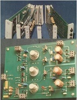
Electronics Control Design Service
Price: 3500 INR/Number
MOQ1 Number
Payment TermsCash on Delivery (COD)
Main Domestic MarketAll India
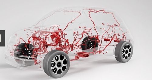
Electronics Design Services - Advanced Hardware Development for Sensors Actuators and Controllers | Comprehensive Engineering Support and CAD/CAE Expertise
ComplianceISO 9001
ComponentsSensors Actuators
DeliverablesSchematics PCB
Design ToolsCAD/CAE
ExpertiseAutomotive
FeaturesExpert Design Quality Assured Rapid Prototyping Production Support Cost Effective
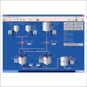
Electronics Scada Designing Services
ComplianceIEC 61131-3
FeaturesSystem design Process control Data analysis Real-time monitoring Efficient operation Cost reduction Improved productivity
HardwareIndustry standard
IntegrationSeamless integration
InterfaceUser-friendly
ScalabilityHighly scalable
Electronics Design Services - Premium Quality Materials Cutting-Edge Technologies | Custom Solutions for Diverse Client Needs
Compliance StandardsIPC-A-600
Design SoftwareAltium Eagle
FeaturesCircuit Design PCB Layout Prototyping Testing Manufacturing Support
Manufacturing ProcessSMTTHT
PCB MaterialFR4
Project ManagementAgile
Hermes Electronics Pvt. Ltd.
Navi Mumbai
Electronics Design Services
ComplianceRoHS
DimensionVaried
FeaturesPCB design Hardware design Software dev System testing Cost effective Latest technology Design optimization Embedded software Mobile apps
LayersMultiple
ManufacturingSMT
MaterialFR4

Electrical Engineering Design
MOQ1 Unit/Units
Payment TermsCash in Advance (CID) Cheque Cash Advance (CA)
Supply Ability30 Per Month
Delivery Time1 Months
Electronic Design Automation Services
Compliance StandardsIndustry Standard
Design MethodologiesVarious
Experience LevelExtensive
FeaturesPCB Design VLSI Design Embedded Systems Real-time apps Faster Prototyping Cost Reduction Improved Designs
Project SizeVariable
Software UsedMultiple
Process Development And Design Service
Design StandardsASME API
FeaturesProcess Design Flow Diagrams Expert Team Cost-Effective Material Selection Equipment Layout Plant Design
Industry FocusManufacturing Chemical
Project Delivery2-6 months
Service TypeProcess Development
Software UsedAspen Plus HYSYS
FAQs Related to Electronics Design Process In Mysuru
How many electronics design process products are available in Mysuru?
Where can I find electronics design process nearby Mysuru?
Can I trust the Mysuru Based Electronics Design Process suppliers listed on Tradeindia?
How many Mysuru based Electronics Design Process manufacturers are there?
What is the price range of electronics design process in Mysuru?
| Company Name | Currency | Product Name | Price |
|---|---|---|---|
| - | - | Electronics Control Design Service | 3500 INR (Approx.) |
| - | - | ELDR Electronic Listening Device | 3999 INR (Approx.) |
| - | - | Electrical Layout Design Service | 2000.00 INR (Approx.) |
What is the delivery time for electronics design process in Mysuru?
Electronics Design Service
ComplianceIEC
Design TypeCustom
FeaturesExpert design Cost effective Fast turnaround High quality
MethodologyAgile
PrototypingAvailable
RevisionsMultiple
Plug In Electronics Design And Fabrication
ComplianceCustom
DimensionsVariable
Dominant ColorGreen
FeaturesCustom Design Reliable Operation High Quality Bulk Supply Import Substitute
MaterialFR4
Number of ComponentsVariable
System Advance Technologies (p) Ltd
Kolkata
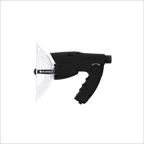
ELDR Electronic Listening Device
ColorBlack
ConnectivityWireless
FeaturesLong Range 8x Zoom Wireless Easy Use Discreet Clear Audio Digital Recorder
Headphone Jack3.5mm
Magnification8X
Power Source9V Battery
Iprealm Technologies Private Limited
Sector 63, Noida
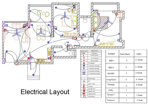
Electrical Layout Design Service
ComplianceNEC
DeliverablesDigital Drawings
FeaturesDetailed Design Efficient Planning Cost Savings Safe Installation Compliance Adherence
FormatPDF DWG
RevisionsUnlimited
Scale1:50

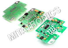
All Electronics Product Design And Development
ComplianceRoHS
DimensionsVariable
FeaturesImproved sales Boosted loyalty Reduced complaints Stronger identity Time reduction Improved efficacy Advanced features Functional safety
Layers2-10
Manufacturing ProcessSMT/THT
MaterialFR4
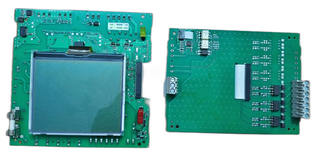
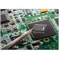
Hardware firmware PCB Design & Development
MOQ1 Piece/Pieces
Charging VoltageIf battery powered: 3.7V/5V/12V supported
InterfaceUART SPI I2C USB CAN
UsageIndustrial automation customized electronics
Power SupplyDC supply
ComponentsMicrocontroller sensors regulators connectors
Response TimeTypically <10ms
Design Of Layout Service
Design TypeMultilayer
FeaturesPCB design Multilayer support Cost effective EDA tools High end
Layers1-12
MaterialFR4
Size RangeCustom
Software UsedEDA
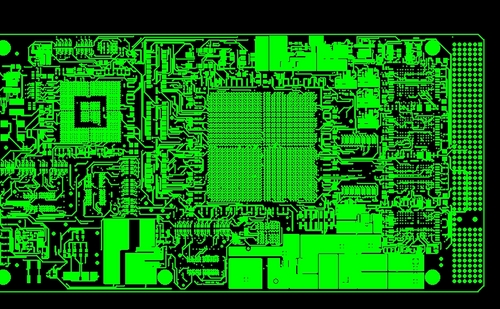
Micro CAD Services PCB - Advanced HDI & Multi-layer Designs | High-Speed Digital RF Analog Signal Integrity Solutions
ComplianceIPC-A-600
Design SoftwareAltium Eagle
FeaturesHDI Designs High-speed PCBs Custom Designs Signal Integrity Fast Turnaround Expert Support Cost-Effective Reliable Service
Layers2-32+
ManufacturingIPC-A-600
MaterialsFR4 Rogers

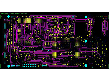
PCB Design Services - Advanced Material Solutions Multi-Layer High-Speed Designs | HDI RF & Analog Expertise Low EMI Applications Complete Assembly Drawings
ApplicationsDiverse
ComplianceIndustry Standards
Design SoftwareTop Tier
FeaturesHDI Designs High-speed PCBs Analog Design SMT Designs Flex PCBs EMI Reduction Assembly Drawings ICT Data
Layer CountMulti-layer
MaterialsAdvanced
High Speed Pcb Design
ComplianceRoHS
FeaturesHigh Speed EMI/EMC Signal Integrity Customizable Cost-effective
Frequency>300 MHz
LayersMultiple
MaterialFR-4
SizeVariable
PCB Design 10 layer
ComplianceIPC-6012
DimensionsVariable
FeaturesMultilayer Design High Reliability Customizable Complex Circuits Military Grade Industrial Use
Layers10 Layers
MaterialFR4
Surface FinishHASL
PCB Design Circuit Board
ComplianceIPC-A-600
DimensionsVariable
FeaturesCustom Design High Reliability Multi-layer Options PCB Assembly Signal Integrity Thermal Analysis
Layers1-12
MaterialFR-4
Surface FinishHASL

PCB Design Inner layer
DimensionsCustomizable
FeaturesHigh Quality Versatile Design Reliable Performance Military Grade Industrial Grade
LayersMulti-layer
MaterialFR4
StandardsIPC-A-600
Thickness1-10mm
PCB Design (Legend/Silkscreen)
ComplianceIPC-2221A
Design SoftwareVarious
FeaturesPrecise Design High Accuracy Customizable Reliable Cost-Effective Scalable Durable Easy-to-use
File FormatGerber
Layers1-Multilayer
Minimum Trace Width5 mil
Staircase Chandeliers - Premium Grade Raw Material Elegant Design | Strictly Tested for Quality Assurance
DimensionsVariable
FeaturesElegant Design Luxury Lighting Energy Efficient Durable Material Easy Installation Modern Style Crystal accents
FinishChrome
MaterialCrystal Metal
StyleModern
VoltageVariable
Popular Categories in Mysuru
Popular Products


© 1999-2026 Infocom Network Private Limited. All rights reserved.