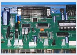
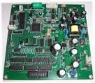
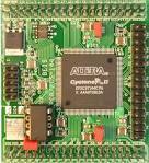
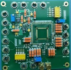
Pcb Layout Design - High-speed, Multi-layer, 30 Layer Ipc Compliant | Advanced Signal Integrity Analysis, Impedance Control, Ultra High Density
Price:
Get Latest Price
In Stock
Product Specifications
| Analysis | Signal, Power, Thermal |
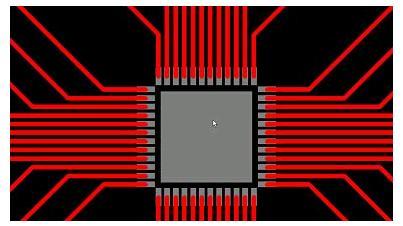
| BGA | 0.5mm pitch |
| Features | High-speed design, Multi-layer PCB, Fast turnaround, High quality, Cost effective |
| Layers | Up to 30 |
| Software | Mentor, Cadence |
| Speed | 2.5Gbps |
| Standards | IPC, UL, MIL |
| Usage | Electronic device prototyping, production |
Product Overview
Key Features
We have established standards for acceptance and delivery which results in faster turnaround time with least error.
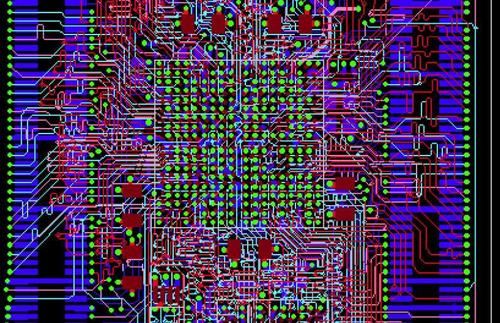
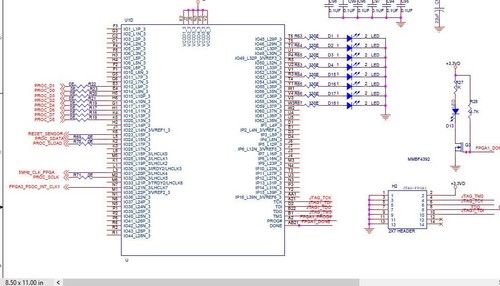
Our PCB Design environment uses best in industry tools like Mentor Graphics and Cadence for design capture, PCB layout and design analysis.
We are customer centric and deliver high quality multi layer high-speed PCB designs, taking into consideration of real-world manufacturing and test requirements. Our PCB design capabilities includes:
* High degree of Expertise in High speed PCB designs.
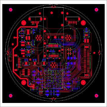
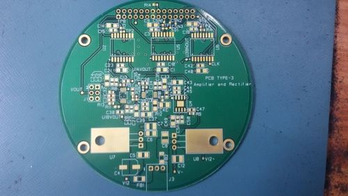
* High speed digital, Analog, mixed digital/analog, RF designs.
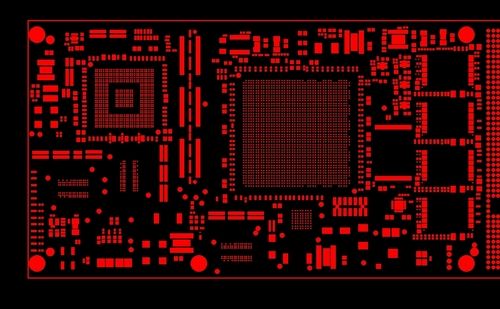
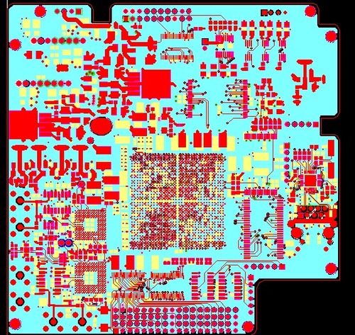
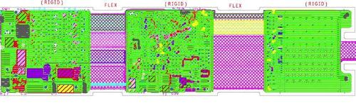
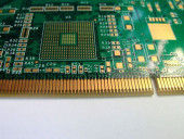
* High Layer count (30 layers), Ultra High density designs.
* Impedance controlled Designs with delay matching, Stack-up and material selection.
* Standards Compliant (IPC, UL, MIL, DO-254) designs as per customer specifications.
* High speed interconnects : 2.5Gbps.
* Multiple Fine pitch BGA (0.5mm) of high pin count(1136).
* Designs with Micro Vias, Blind Vias, Buried Via and back drill.
* Motherboards, Single Board computers, High speed Serial Back planes, Telecom Backplane.
* ASIC Test Boards, Load Boards, Probe Cards, Burn-in Boards, sockets, Package Design.
* Pre-Route and post-route Signal Integrity Analysis, IBIS Model Creation.
* Cross talk analysis, Timing analysis, EMI analysis, Power Integrity analysis.
* Board and system Level Thermal Design, simulation and analysis, Multi-board analysis.
Company Details
We firmly believe in First time right designs Every design is well thought over. They pass through an exhaustive checklist process to ensure most of the errors are trapped and Resolved on the first go. Because of this checklist process, there is a huge saving time & costs. Most of our PCB designs end up being right the first time that can be taken into production straight away. Argus Technologies is in business since May 2008. The rich experience gained over those years in various fields of electronics design, software, prototyping & manufacturing, Advance PCB testing, PCB assembly printed circuit Boards,PCB Fabrication is a huge advantage. We served our Product designs to our clients allover India. We design electronic products, from concept to completion by using best PCB testing tools for board printing. Being a design firm based in Hyderabad, Bangalore, and Chennai, India & due to the immense talent pool with low operating costs customers can expect quick, responsive & quality service. Our motto is to work with customers who are looking to outsource their design, programming & manufacturing to lower costs & improve quality levels. Argus Technologies focus towards customized their designs to achieve low manufacturing costs, with carefully chosen low-cost components, without compromising on quality, while offering excellent support in the projects. We believe in ÃA ¢ÃA ÂA ÃA ÂA keeping things simpleÃA ¢ÃA ÂA ÃA ÂA hence, the costs are low while maintaining high-Quality standards. We not only offer electronic design services, PCB Design, PCB manufacturing, PCB Fabrication , PCB Layout, Printed circuit Board design but also support our customers in prototyping and Using PCB testing methods, low volume & high volume manufacturing services. Argus offers best Electronic Product design services and complete Contract Electronic manufacturing services. An Experienced technical team with a wide spectrum of skills on different platforms and various industry domains helps to reduce development risk and offer cost and time to market advantage.
Business Type
Exporter, Manufacturer, Service Provider, Supplier
Employee Count
50
Establishment
2011
Working Days
To
GST NO
36ALSPM8596Q1ZL
Payment Mode
Cheque, Days after Acceptance (DA), Telegraphic Transfer (T/T)
More Products From This Seller


Seller Details
GST - 36ALSPM8596Q1ZL
Hyderabad, Telangana
Director
Mr. Pradeep Kumar
Address
Plot No. 38, Phase-III, 2nd Floor, Kamalapuri Colony Hyderabad, Telangana, 500073, India
Report incorrect details