

Pcb Design Services In Bhopal
(108 products)
PCB Designing Service - Glass Epoxy Paper Finolic Multi-layer up to 3.6 Micron Cladding Thickness | Expert Circuit Design to PCB Conversion
LayersSingle-Multi
MaterialGlass Epoxy
ThicknessUp to 3.6 micron
DesignCircuit to PCB
ConversionPCB to Circuit
UsagePrototyping production runs of electronic devices or custom projects.
Commercial Pcb Design Services
Price: 20000.0 INR/Unit
MOQ1 Unit/Units
FOB PortINDORE
Payment TermsCash Advance (CA)
Supply Ability2 Per Week
Rapid Automation Sales And Services
Indore

PCB Design Development Services
Design SoftwareCAD/CAM
Service ContractProject-based
Turnaround Time2-3 days
PCB MaterialFR4
ColorGreen
UsageAudio amplifier circuit design

Full Custom PCB Design Services
Design TypeFull Custom
MaterialFR4
Layers2-10
Surface FinishHASL
Minimum Track Width5 mil
UsagePrototyping and low-volume production
PCB Designing And Circuit Designing Service
SoftwareCAD/CAM
Design TypeCustom
Service TypeProject-based
Minimum Charge2500 INR
Minimum Order1 project
RevisionsMultiple
Multilayer PCB Design Services
Price: 3000 INR/Unit
MOQ10 Unit/Units
FOB PortVADODARA
Payment TermsPaypal Cash on Delivery (COD) Cash Advance (CA)
Supply Ability1000 Per Month
PCB Designing Services - Advanced Design Techniques Skilled Professionals Compliance with International Quality Standards
SoftwareAltium Eagle
Design ComplexityHigh
Layers4-16
Manufacturing MethodSMT THM
MaterialFR4
ComplianceIPC-A-600
Leons' Integrations Private Limited
Gotri Road, Vadodara

PCB Designing Service - Multilayer Double Side & Single Side | Fast Turnaround Cost-effective Solutions Post-release Updates Schematic Verification DRC Compliance
Layers1-12
MaterialsFR4 Rogers
SoftwareAltium Eagle
Turnaround1-4 weeks
ComplianceIPC-2221
Design TypesSingle Double Multilayer

PCB Design Services - Premium Quality Innovative Technology Utilization Guaranteed Excellence
Design SoftwareAltium Eagle
Layers2-16
MaterialFR4 Rogers
SizeCustom
ManufacturingLocal
UsagePrototyping Production OEM
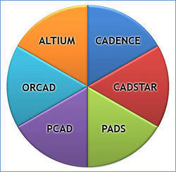
Pcb Design Expertise Service
SoftwareAltium Cadence Orcad Cadstar Pads PCAD
Experience LevelExtensive
CertificationIPC Certified
Revision ControlGit
Design StandardsIPC-2221 IPC-7351
Delivery TimeProject-Specific
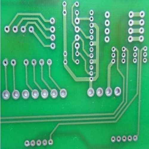
Double Layer PCB Design Service
LayersTwo
MaterialFR4
DimensionsVariable
Trace Width10mil
Spacing10mil
ComplianceRoHS
PCB Design Services - Tailored Offline Solutions Flexible Duration | Comprehensive PCB Design Expertise
Design SoftwareAltium Eagle
MaterialFR4
Layers2-8
Thickness1.6mm
Surface FinishHASL
UsagePrototype and production PCB design
FAQs Related to Pcb Design Services In Bhopal
How many pcb design services products are available in Bhopal?
Where can I find pcb design services nearby Bhopal?
What are some related categories to pcb design services in Bhopal?
Can I trust the Bhopal Based Pcb Design Services suppliers listed on Tradeindia?
How many Bhopal based Pcb Design Services manufacturers are there?
What is the price range of pcb design services in Bhopal?
| Company Name | Currency | Product Name | Price |
|---|---|---|---|
| - | - | Commercial Pcb Design Services | 20000.0 INR (Approx.) |
| - | - | Full Custom PCB Design Services | 250 INR (Approx.) |
| - | - | PCB Designing And Circuit Designing Service | 2500 INR (Approx.) |
| - | - | Multilayer PCB Design Services | 3000 INR (Approx.) |
What is the delivery time for pcb design services in Bhopal?

PCB Design Services - 1.2 MM Glass Epoxy Material | High-Quality Circuit Boards with Rapid Prototyping and Compliance to Industry Standards
Thickness1.2 mm
MaterialGlass Epoxy
UsageCircuit board design for manufacturers
SoftwareAdvanced tools
TeamExperienced engineers
ComplianceIndustry standards
PCB Designing Services - Superior Quality Designs | Affordable Pricing Expert Team
Design SoftwareAltium Eagle
PCB MaterialFR4
Layer Count2-16 layers
Minimum Trace Width5 mil
Minimum Spacing5 mil
Manufacturing ProcessCNC Milling
CAD Design Service - Project Based Solutions | Innovative CAD/CAM Techniques for Manufacturing Excellence
SoftwareAltium
Design TypeMultilayer
Layers6-12
SizeVariable
MaterialsFR4
UsageManufacturing process improvement prototype creation production optimization
CAD-CAM for PCB Designing Service
SoftwareCAD/CAM
Design TypeSingle/Multilayer
LayersUp to 16
ComplianceIPC standards
OutputGerber files
UsagePCB design and manufacturing services in Gandhinagar Gujarat India creating single-sided double-sided and multilayer PCBs from schematic to final layout.
Black Pcb Designing Services
SoftwareAltium Eagle
Layers2-30+
TechnologySMT TH
Design RulesIPC-2221
DeliverablesGerber Files
UsagePCB layout and schematic design for electronics manufacturing. Includes custom component placement and routing.

PCB Design Services - IPC Compliance Layer Stack Management & Impedance Controlled Trace Simulation | Timely and Expert Solutions
Design SoftwareAltium Eagle
Layers2-16+
Trace Width5-50 mil
Impedance ControlYes
SimulationYes
UsagePrototypes small-medium batch production runs custom designs electronic devices
PCB Designing Service - High Efficiency Solutions | Timely Execution Concept Development Reliable Expertise
Design SoftwareAltium Eagle
Layers2-20+
File FormatsGerber ODB++ IPC-2581
ManufacturingSurface mount
ComplianceIPC-A-600
UsagePrototyping production custom circuit boards

Hardware And PCB Designing Services
Design TypeEmbedded Hardware
ProcessorsARM TI Intel
MicrocontrollersTI Atmel NXP
FPGA/CPLDXilinx/Altera
CommunicationUSB Ethernet Serial
UsagePCB & Hardware design for custom embedded systems

Pcb Layout Design Services
SoftwareAltium Cadence
Design TypesHigh-speed Analog
Layers4-32+
TechnologyHDI Stacked via
AnalysisSI PI EMC
ComplianceIPC-2221A

Pcb Design Training Service
Course Duration2 Months
CertificationYes
Software UsedOrcad
Course Modules6
LocationAhmedabad Gujarat
Target AudienceFreshers
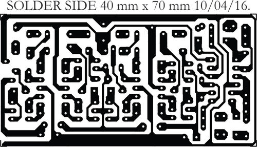
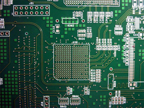
PCB (Printed Circuit Board) Designing Services
Dimensions40mm x 70mm
MaterialFR4
Layers2
Thickness1.6mm
Surface FinishHASL
Trace Width0.1mm

PCB Designing Service - Expertly Crafted Designs | Superior Quality Affordable Pricing Experienced Team Members
Design SoftwareAltium Eagle
Layers2-30+
MaterialFR4Rogers
Trace Width5-50mil
Spacing5-50mil
UsagePrototypingproduction runs

PCB Designing Services - Expert Layout Solutions | Best in Class Design for All Your Needs
Design SoftwareAltium
MaterialFR4
Layers2-layer
Thickness1.6mm
Size RangeCustom
Surface FinishHASL

PCB Layout Services
SoftwareAltium Eagle
Design RulesIPC-2221A
Layers2-32 layers
Turnaround Time1-4 weeks
Revisions2-3 included
UsagePCB design for prototypes production and custom applications.
PCB CAM Design Services
SoftwareCAM/CAD
Design typePCB
File formatsMultiple
RevisionsUnlimited
Turnaround time1-3 days
UsagePCB manufacturing design & layout in Surat
Popular Categories in Bhopal
Popular Products


© 1999-2025 Infocom Network Private Limited. All rights reserved.