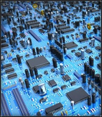
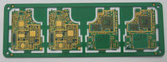
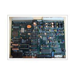
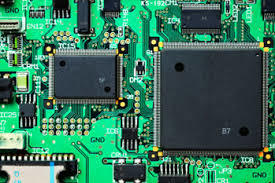
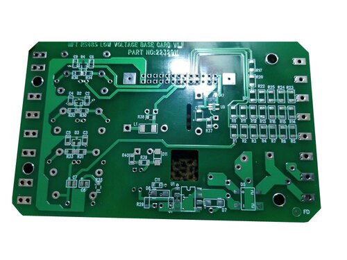
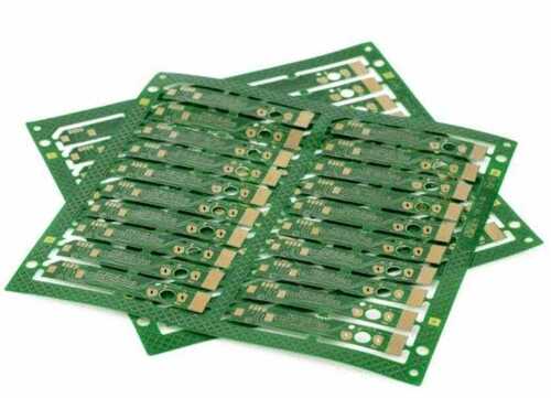
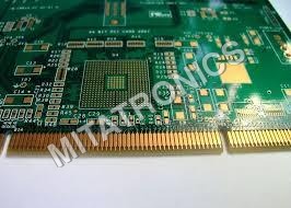
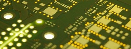
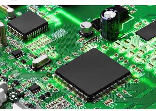
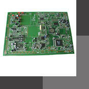
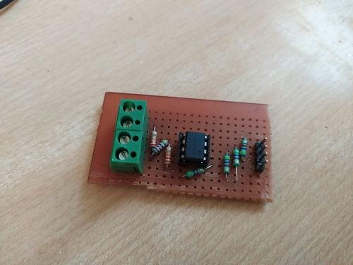
Full Custom Pcb Design Services
Price: 250 INR / Piece
Get Latest Price
Minimum Order Quantity :
1 Piece
In Stock
Product Specifications
| Compliance | RoHS |
| Design Type | Full Custom |
| Features | Custom design, Fast turnaround, Cost effective, Hassle free |
| Layers | 2-10 |
| Material | FR4 |
| Minimum Track Width | 5 mil |
| Surface Finish | HASL |
| Usage | Prototyping and low-volume production |
| Payment Terms | Cash on Delivery (COD), Others, Cash Against Delivery (CAD), Cash in Advance (CID), Cheque, Cash Advance (CA) |
| Supply Ability | 50 Per Day |
| Delivery Time | 4 Week |
| Sample Available | Yes |
| Sample Policy | Free samples are available |
| Main Domestic Market | All India |
Product Overview
Key Features
Effective : Yes
Service mode : Offline
Services Charges : Reasonable
Hassle Free Service
Company Details
Business Type
Service Provider
Employee Count
1
Establishment
2019
Working Days
To
Payment Mode
Cash Advance (CA)
Related Products
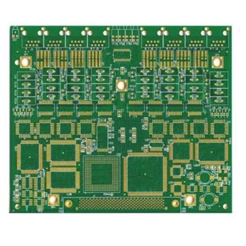
Multilayer PCB Assembly - FR4 Material, Customizable Thickness & Trace Width | Compact Design, High Reliability, Improved Shielding, Reduced Errors
Sunanda Enterprises
Navi Mumbai, Maharashtra
Multilayer Pcb Board - Base Material: Cem2
Price: 10.00 INR
MOQ - 5000 Unit/Units
Ishwari Global Tech Pvt Ltd
Amravati, Maharashtra
Multilayer Pcb - FR4 Material, 1 Layer, Green | Good Quality, 1 Year Warranty
Price: 50 INR
MOQ - 1000 Piece/Pieces
Asha Electronics
Pune, Maharashtra
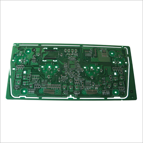
Multilayer PCB - FR4, 4-12+ Layers, 1.0-3.0 mm Thickness, Variable Dimensions | RoHS Compliant, HASL Surface Finish, Ideal for Electronics Manufacturing and Industrial Applications
Mohite Electronics Private Limited
Pune, Maharashtra
Light Weighted Heat-Resistant Plastic Body Electronic Multilayer PCB
Price: 1000 INR
MOQ - 50 Piece/Pieces
Asps Sales Services & Enterprises
Bhosari, Maharashtra
Multilayer Pcb - Aluminum, 1.55mm Copper Thickness, Green Solder Mask, 0.20mm Hole Size | Flexible Board, Lead Free Surface Finish, Flying Probe Test
Price: 50 INR
MOQ - 100 Piece/Pieces
Ropes Tech Pvt. Ltd.
Pune, Maharashtra
Multilayer PCBs - High-Quality, Customizable Designs | Time and Cost Efficiency, Reduced Workload
Wurth Electronics Services India (p) Ltd.
Pune, Maharashtra
Multilayer Pcb Assembly
Price: 0.75 INR
MOQ - 5000 Piece/Pieces
Electrotrail Technologies Pvt. Ltd.
Pune, Maharashtra

Multilayer PCB - Advanced Multilayer Technology, 21000 SQM Facility Space, Operational Excellence
Epitome Components Ltd.
Ahilyanagar, Maharashtra
Explore Related Categories


More Products From This Seller
Seller Details
Aurangabad, Maharashtra
Electrical & Electronics Design Engineer
Mr Mihir Karkhane
Address
N-1 230/F, Chhatrapati Sambhajinagar, Maharashtra, 431003, India
multilayer pcb in Aurangabad
Report incorrect details