Black-brown-honey Pcb Design And Layout Services
Price:
Get Latest Price
In Stock
Product Specifications
| CAD | AutoCAD |
| Compliance | IPC standards |
| Design Rules | High-speed |
| Features | Expert Design, Cost Savings, Fast Turnaround, Accurate Designs, Functional Boards |
| Layers | Multi-layer |
| Output | Gerber Files |
| Software | Protel, OrCAD |
| Usage | Electronic circuit design and PCB layout for diverse applications. |
Product Overview
Key Features
PCB Design and Layout Services
We are one of the best Service Provider, our company is based in Karnataka, India, offering PCB Design and Layout Services. We ensure that our boards are designed to reduce and eliminate a second iteration, as multiple iterations are expensive and time consuming. Our company has a team of experts, they make sure you get superlative PCB designs. We have wide experience of providing functional and accurate PCB Design and Layout Services solution. All the customers can avail the benefit of our services at market leading price.
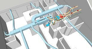
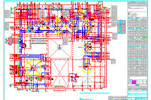
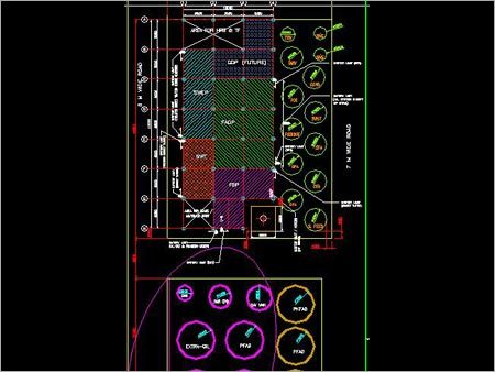
CADTRANS is engaged in offering PCB Design and Layout Services that are tailor made especially for organizations with rudimentary infrastructure. We assist in upgrading electronic designs for our customers within a specific time. We utilize advanced programming languages like Protel and Or Cad to design printed circuit board. The application of AutoCad enables us to represent the PCB's mechanical characteristics. We are proud for having expertise in other CAD programs that are necessary for apprehension of net list data. Our responsibilities, abilities and execution process of services include
Design for Fabrication Services:
- Creation of electronic circuit design
- Preparing list of raw materials
- Producing CAM data, board artwork and SMT solder paste stencil artwork
- Differential pairs, high speed rules, multi-layer boards, split ground planes
- Clearance rules, keep-out, routing per trace/space as demanded by clients
- Rearrangement of components as per data regarding reverse annotation to diagram and physical layout
Design for Test Service:
- Conduct auditing work
- Producing test result
- Examination and approval of test probe as required by clients
- Preparing documents of test
Documentation:
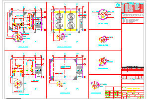
- Preparing documents on circuit board foil layers, overlay screening layers and solder mask layers
- Representation of schematic drawings
- Bill of materials
- Assembly drawings, fabrication drawing, fabrication panel drawings
- CAM X-Y data file, SMT stencil artwork
- PDF file containing drawings necessary for preparing computer program
- Generation of excel files, Gerber files and text
- Preparation of CAD database files
Company Details
Business Type
Service Provider
Employee Count
10
Establishment
2012
More Products From This Seller


Seller Details
Bengaluru, Karnataka
CEO
Ms. Saritha Kannan
Address
No.1, First Floor, 10th Main, 2nd Cross, Nandanam Colony, Bengaluru, Karnataka, 560043, India
pcb design services in Bengaluru
Report incorrect details