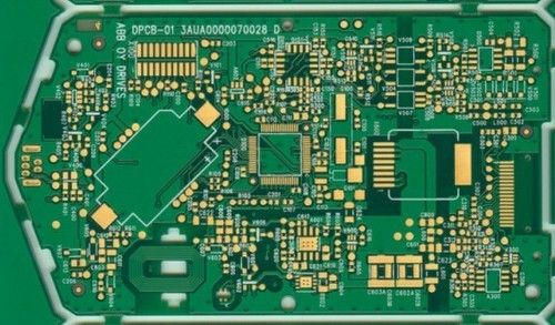
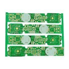
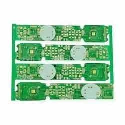
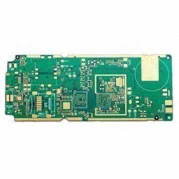
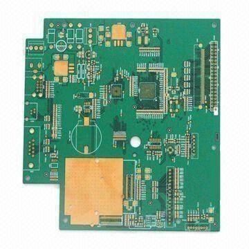
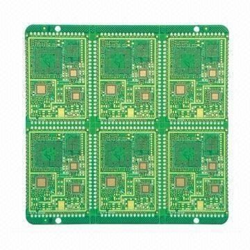
Four Layer Pcb With Immersion Gold Surface Treatment
Price:
Get Latest Price
In Stock
Product Specifications
| Layers | Four |
| Material | FR4 |
| Copper | 1oz |
| Hole Size | 0.3mm |
| Line Width | 0.35mm |
| Thickness | 1.6mm |
| Surface Finish | Immersion Gold |
| Features | High Reliability, Long Lifespan, Cost-effective, Immersion Gold, Four Layers, High Density, Quick Turnaround |
Product Overview
Key Features
Layer count: four
Base material: FR4 (Tg150)
Copper thickness: 1oz
Minimum hole size: 0.3mm
Minimum line width/space: 0.35mm
Solder mask: glossy green/10 to 30um
Blind buried holes: supported
Controlled impedance: supported
Surface treatment: immersion gold
Finished board thickness: 1.6mm
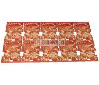
Panel array: five pieces in one panel
Profile: CNC routing and v-cut
Company Details
Focusing on a customer-centric approach, Shenzhen 3c-technology Co.,Ltd has a pan-India presence and caters to a huge consumer base throughout the country. Get Circuit Boards from Shenzhen 3c-technology Co.,Ltd at Trade India quality-assured services.
Business Type
Exporter, Service Provider, Supplier
Establishment
1998
Related Products
Gold Plated Domes Used Membrane Keyboard - Membrane Type | Innovative Design, Higher Efficiency, Low Maintenance, Customizable Sizes
Price: 12 INR
MOQ - 500 Inch/Inches
Feather Graphics India Pvt. Ltd.
Ghaziabad, Uttar Pradesh
Gold Plated PCB - CNC Drilled, Multi-Layer Design | Hot Air Levelling & OSP Surface Finishing
Om Circuit Boards
Ghaziabad, Uttar Pradesh
Gold Plated PCB - Multi-Layered Gold Plated Circuit Boards | CNC Drilled, Hot Air Leveling, OSP Finishes
Chem-equip
Nashik, Maharashtra
Explore Related Categories


More Product From This seller


Seller Details
Shenzhen, Guangdong
Mr. Adam Chen
Address
Rm. 502, Xinbaosheng Bldg., 233 Xixiang Rd., Xixiang, Bao'an, Shenzhen, Guangdong, 518102, China
gold plating pcb in Shenzhen
Report incorrect details