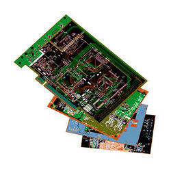
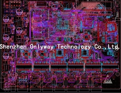
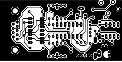
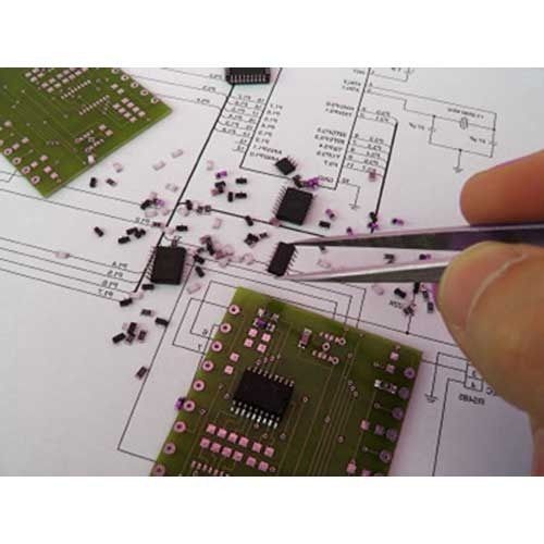
Cad Pcb Layout Design
Price:
Get Latest Price
In Stock
Product Specifications
| Design Rule Check | Yes |
| Features | Expert Design, Fast Turnaround, Cost-Effective, Advanced Tech, PCB Layout, Reliable Service |
| Layer Count | 4-16 layers |
| Manufacturing Process | SMT |
| Revision Control | Git |
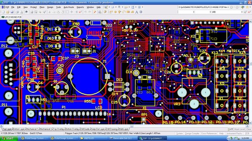
| Software | Altium Designer |
| Turnaround Time | 1-3 days |
| Usage | PCB design for electronics |
Product Overview
Key Features
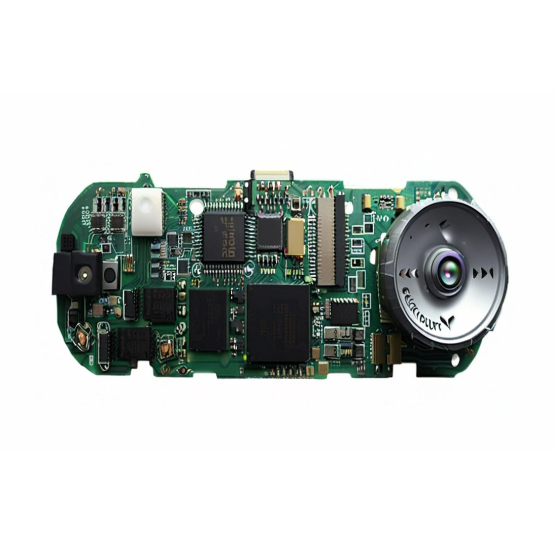
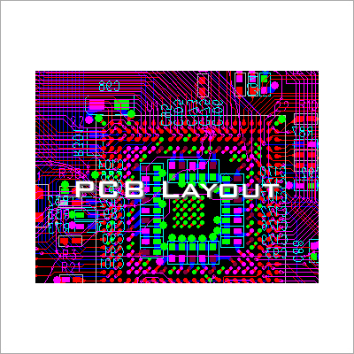
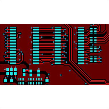
CAD PCB Layout Design Services
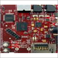
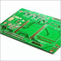
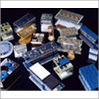
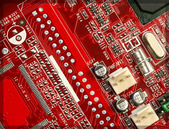
Being quality based company we are providing CAD PCB Layout Design services as per current technology. We are using advanced technology during this PCB layout designing work. We have with us expert technicians, who posses rich knowledge in this domain. We are committed to offer these layout designing services within stipulated time frame. We are providing these services for electrical and electronic industries. Apart from this, clients can avail CAD PCB Layout Design services from us at reasonable charges.
Company Details
Business Type
Exporter, Manufacturer, Service Provider, Supplier
Employee Count
58
Establishment
1995
Related Products

Shenzhen Professional Customized PCB Layout Assembly PCBA Electronic Circuit Board supplier electronic parts design service
Nova Technology Vietnamese Company Limited
Ho Chi Minh City, Thanh Pho Ho Chi Minh

PCB Layout Computer Aided Design - Multilayer, 2-16 Layers, CAD & Gerber File Formats | Expert Team, Fast Service, High Production Volume
Asha Electronics Pvt. Ltd.
Mumbai, Maharashtra
PCB Layout Design - Single & Double Sided PCB Design, Advanced Schematic Capture and Board Layout Services
Nexfy Embedded Technology
Ahmedabad, Gujarat

PCB Layout Service - Altium Design, Multiple Layers, Gerber Files | Fast Turnaround, Accurate Layouts, Version Control
I Global Tech
Ahmedabad, Gujarat
Explore Related Categories


More Products From This Seller


Seller Details
New Delhi, Delhi
Name
Mr. Dinesh Daksha
Address
6/9, Gate No-3, Ist Floor, Industrial Area, Kirti Nagar, New Delhi, Delhi, 110015, India
Report incorrect details