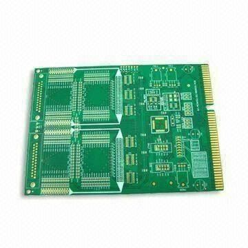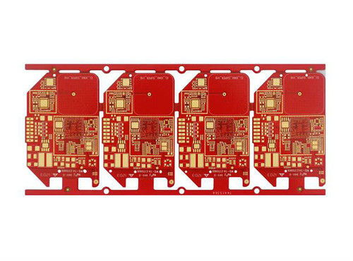
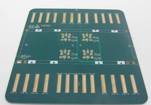
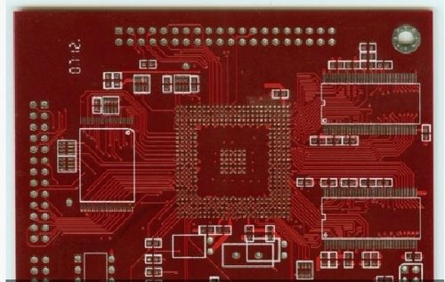
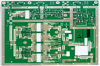
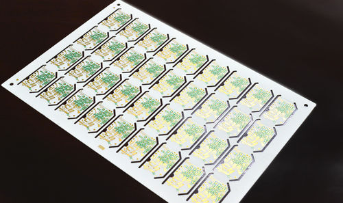
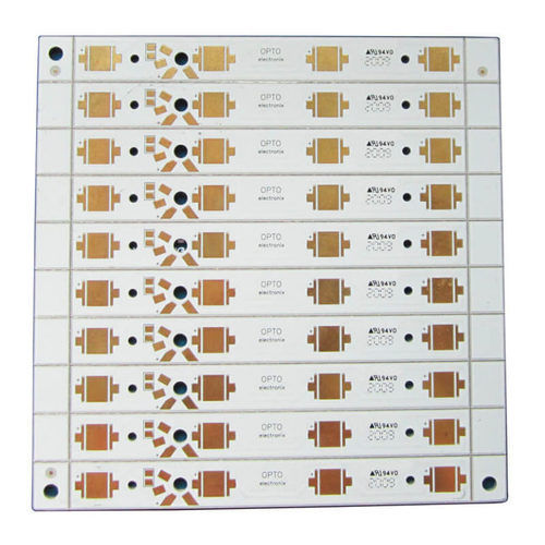
4 Layer Fr4 Enig+osp Pcb - 1.6 Mm Thickness, Red Soldermask, 0.3 Mm Min Hole Size | Rigid Design, 1 Oz Copper, 94 V-0 Flame Resistance, 200x250 Mm Panel Size
Price:
Get Latest Price
In Stock
Product Specifications
| Soldermask | Red |
| Hole Size | 0.25 Millimeter (mm) |
| Min. Line Spacing | 0.2 Millimeter (mm) |
| Silkscreen | White |
| Flame Resistance Level | 94 V-0 |
| Board Type | Rigid |
| Min. Line Width | 0.15 Millimeter (mm) |
| Test | E-Test |
| Base Material | FR4 |
| Surface Finish | ENIG |
| Copper Thickness | 1 OZ Feet (ft) |
| Board Thickness | 1.6 Millimeter (mm) |
| Color | Red |
| Panel Size | 200*250 |
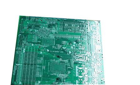
| Number Of Layers | 4 Layer |
| FOB Port | Yantian |
| Payment Terms | Cash on Delivery (COD), Cash Advance (CA), Letter of Credit (L/C), Western Union, Paypal, Cash Against Delivery (CAD), Telegraphic Transfer (T/T), Others, Delivery Point (DP), Days after Acceptance (DA), Cash in Advance (CID), Cheque |
| Delivery Time | 5 Days |
| Sample Available | Yes |
| Sample Policy | Free samples are available |
| Main Export Market(s) | Western Europe, Asia, Australia, South America, Eastern Europe, Middle East, Central America, North America, Africa |
| Main Domestic Market | All India |
Product Overview
Key Features
Thickness: 1.2+/-0.12 mm
Min Hole Size: 0.3 mm
Width/Space: 0.12mm/0.12 mm
Surface Treatment: ENIG
Craft :
Red Ink
ENIG+OSP
Application :
Consumer Electronics
Company Details
Business Type
Exporter, Manufacturer, Service Provider, Supplier
Employee Count
753
Establishment
2001
Working Days
To
Payment Mode
Cash on Delivery (COD)
Certification
ISO 9001:2008
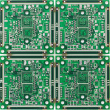
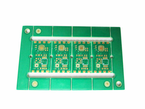
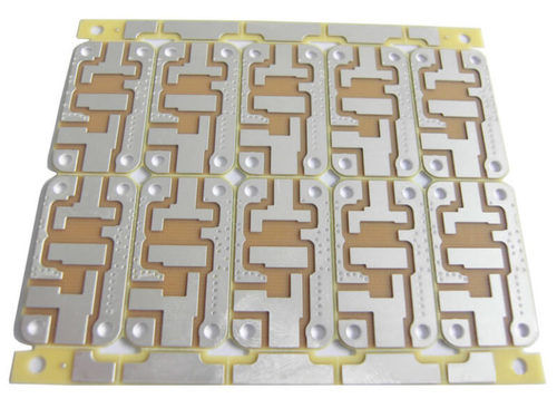
Related Products
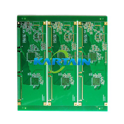
Multilayer Pcb Circuit Board - Base Material: Alumunium
Price: 10 USD ($)
MOQ - 100 Unit/Units
Kartain Technology Co., Ltd.
Shenzhen, Guangdong


Professional Multi Layer Oem Fr4 Pcb Circuit Board
Airuida Technology Co., Limited
Shenzhen, Guangdong
Multilayer PCB - High Grade Material, Custom Specifications for Versatile Applications
Andwin Circuits Co.,ltd
Shenzhen, Guangdong

Multilayer PCB - High Precision, High Density Engineering | Custom Sizes and Specifications
E T Limited
Shenzhen, Guangdong

Multilayer PCB - Aluminum Base, 0.6-5mm Thickness, 0.5-4 OZ Copper, 50-250V E-Test Voltage | High Thermal Conductivity, Various Surface Finishes
Shenzhen Kerui Electronic Industry Co.,ltd
Shenzhen, Guangdong
Explore Related Categories


More Products From This Seller
Seller Details
Shenzhen, Guangdong
Address
No 2013, Zhijian Time Square, Henggang Town, Longgang District, Shenzhen, Guangdong, 518126, China
multilayer pcb in Shenzhen
Report incorrect details