voice searchcamera search

Wafers In Pusan

(6 products)
Nonelastic Solid Metal Seat Brm Lug (Wafer)

Nonelastic Solid Metal Seat Brm Lug (Wafer)

Design StandardJis, Ansi

Design Pressure5/20

Design Temperature-40~+600

Size80A~1000A

FluidSteam, Oil

BodyDuctile Iron

More details...

Hifly Valve Co.,ltd.

Pusan

Business Type:Manufacturer | Distributor
Established In:2006
PLC Splitter Wafer 1xN, 2xN

PLC Splitter Wafer 1xN, 2xN

MaterialSilica Glass

Wavelength Range1260-1650nm

PDLLow

ILLow

UniformityHigh

PackagingWafer

More details...

Neon Photonics Co. Ltd.

Kwangju

Business Type:Manufacturer | Exporter
Established In:2009
PLC Splitter Wafer - Planar Waveguide Material, 8 Inch Wafer, 1x8/1x16/1x32 Types | Low Insertion Loss, Low PDL, Wide Wavelength Range

PLC Splitter Wafer - Planar Waveguide Material, 8 Inch Wafer, 1x8/1x16/1x32 Types | Low Insertion Loss, Low PDL, Wide Wavelength Range

Size8 inch wafer

MaterialPlanar waveguide

WavelengthWide range

Insertion LossLow

PDLLow

UniformityLow
More details...

P-cube Co,. Ltd

Kwangju

Business Type:Manufacturer
Established In:2009
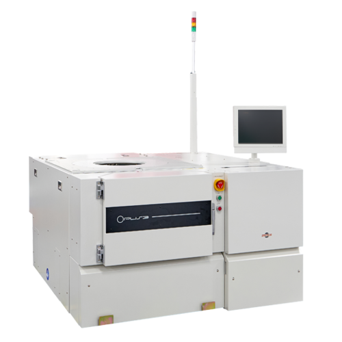
OPUS3 Prober handling SEMI standard wafers

OPUS3 Prober handling SEMI standard wafers

MOQ1 Set/Sets

Operating Temperature15AdegC to 35AdegC

Mounting TypeFloor Standing

Efficiency>95%

Humidity %20% - 80% (Non-Condensing)

Connector TypeSMEMA, USB, RS232

FeatureProgrammable, High Precision, Automated Handler, SEMI-Compliant

More details...

Yesonbiz

Seoul

Business Type:Manufacturer | Exporter
Established In:2000
Wafer Chip Semiconductor - Silicon 10mm Diameter, 0.5mm Thickness | Low Power, Durable, Scalable, ±1% Tolerance

Wafer Chip Semiconductor - Silicon 10mm Diameter, 0.5mm Thickness | Low Power, Durable, Scalable, ±1% Tolerance

MaterialSilicon

Diameter10mm

Thickness0.5mm

Resistance10kΩ

Tolerance±1%

Operating temperature-40°C to +125°C

More details...

Buyersguide

Seoul

Business Type:Trading Company
Wafer Inspection (WIS-1000) - 1500x1000x2000 mm, Line Scan CCD Camera, Hybrid Illumination | Surface Defect 2D, Bump 3D Inspection, Golden Die, Advanced D2D Algorithm

Wafer Inspection (WIS-1000) - 1500x1000x2000 mm, Line Scan CCD Camera, Hybrid Illumination | Surface Defect 2D, Bump 3D Inspection, Golden Die, Advanced D2D Algorithm

Inspection TypeSurface, Bump

Camera TypeLine Scan CCD

IlluminationHybrid

AlgorithmGolden Die, D2D

ThroughputVariable

Dimensions1500x1000x2000 mm (Approx)

More details...

Advanced Technology Inc.

Incheon

Business Type:Supplier | Exporter

FAQs Related to Wafers In Pusan

How many wafers products are available in Pusan?

The range of offered wafers products in Pusan is impressive, with a total of 6 products currently available.

Where can I find wafers nearby Pusan?

You can find wafers around Pusan such as Seoul. You can also use Tradeindia to search for wafers suppliers in Pusan.

Can I trust the Pusan Based Wafers suppliers listed on Tradeindia?

You can use the Trust Stamp feature on Tradeindia to find Pusan Based Wafers suppliers who have been verified as trustworthy. You can also look at the supplier's ratings and feedback from previous customers to help you make an informed decision.

How many Pusan based Wafers manufacturers are there?

There are many wafers manufacturers in Pusan. You can use Tradeindia to search for wafers manufacturers in Pusan and filter your search based on your requirements.

What is the delivery time for wafers in Pusan?

The delivery time for wafers in Pusan can vary depending on the manufacturer and the product. As per the information provided by listed sellers, the delivery time can take up to 1 week for some suppliers.